Photonic Crystal/ Optomechanics
Photonic Quantum Devices And Their Applications
Research topics:Photonic Crystal/ Optomechanics
Photonic Crystal
Photonic crystal exploiting photonic band structures, provides a novel way to guide,control,and manipulate the photons.
Based on photonic crystal waveguides and microcavities, not only the traditional optoelectronic devices with new features, but also the photonic integrated circuits with ultra-compact micro/nano devices can be realized. Our group engages in the research of both passive and active photonic crystal devices and their applications with taking into account two material systems of silicon and InGaAsP. Focusing on the development of photonic integration technology, theoretical design, micro/nano fabrication, and measurement technology have be implemented with breakthroughs.
Optomechanical Crystal (PoXonic Crystal)
Optomechanical crystal cavities based on cavity optomechanics, as a burgeoning field of research in recent years, will lead to breakthroughs in the field of mesoscopic physics and quantum realm.
Localization and manipulation of photons and phonons can be realized by exploiting optomechanical crystal cavities, so that the interaction between photon and phonon can be improved significantly. Thus, the phonons can be annihilated via the energy coupling to photons and macro/meso-scopic quantum ground state can be achieved, wherein the vibration of a system is kept in an “ultracold” vacuum state without phonons. In contrast to the control of atom level objects by Doppler laser cooling, manipulation of the mechanical motion with light spans the size of quantum objects from atomic to macro/meso-scopic scale. So far, using optomechanical crystal cavities is the only possible solution for implementing the on-chip quantum ground state, which will trigger the revolutions in the progress of quantum control, precise measurement and quantum information, etc.
Research Topic:
- Optomechanical crystal cavity
- Photonic crystal waveguide and microcavity
- Slow light and true time delay of photonic crystal waveguide
- Integrated photonic crystal passive device
- Direct modulation of nanocavity light emitting diodes
Representative Results:
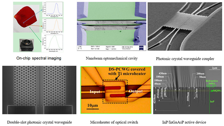
For chip-scale spectrometers, we presented a novel spectral imaging chip with peak position deviation within 1 nm and working bandwidth of 450-750nm.
Radiation-pressure anti-damping-enhanced optomechanical spring-sensing based on a silicon nanobeam optomechanical structure was proposed and demonstrated, which enables a sensing resolution of δλ/λ0 ~ 10?7. (ACS Photonics, 5_4164, 2018)A heterogeneous optomechanical crystal microcavity was proposed and prepared. Different from ordinary optomechanical crystal microcavity, which uses a periodic structure to limit both optical and mechanical modes, this structure uses two periodic regions to limit optical and mechanical modes respectively, and realizes a heterogeneous microcavity structure with an optomechanical coupling coefficient of 1.31 MHz. Experimental tests showed that the mechanical frequency was as high as 5.66GHz. (Scientific Reports, 6: 34160, 2016; Scientific Reports 5: 15964, 2015; Journal of Optics 17(4): 045001, 2015)
A principle of optical switch based on defect modes coupling in photonic crystal waveguide (PCW) is proposed and demonstrated through a W2 PCW (with line-defect width of two rows of missing holes) with integrated titanium/aluminum microheater. Switching functionality with bandwidth up to 24 nm and extinction ratio in excess of 15 dB over the entire bandwidth is achieved by the PCW with footprint of only 8mm×17.6mm, which is the most compact broadband optical switch. (Applied Physics Letters, 95:191901, 2009; Applied Physics Letters, 100: 201102, 2012; Applied Physics Letters, 101: 151110, 2012; IEEE Photonics Journal 5 (2):2200606, 2013)
Air-bridge photonic crystal waveguide (PCW) with slow light effect is demonstrated with a group velocity lower than c/80. A wavelength dependent group delay of 10 GHz sinusoidal microwave signal up to 25±2.5 ps has been implemented with a fabricated 475 mm long PCW. (Chinese Physics Letters, 26 (7):74213, 2009; Chinese Physics Letters, 25(12):4311, 2008)
Etching depth up to 3.5μm and 1.8μm for 200nm-diameter holes and 40nm-width slots are achieved respectively. This is a record-high aspect-ratio of etching in InP heterostructure, and paves the way for ultra-compact InP-based and electrically-pumped optical devices for future mono-/hetero-integrated photonic circuits. (AIP Advances, 3 (2), 022122, 2013) Photonic crystal nanobeam cavity with stagger holes for direct modulation of nanocavity light emitting diodes is proposed. Quality factor of the proposed cavity can be widely engineered while keeping a small mode volume. Simulation result shows a direct modulation bandwidth over 60GHz. (IEEE Photonics Journal, 5(1), 4700306, 2013)